- 您现在的位置:买卖IC网 > Sheet目录1233 > NCP1605LCDTVGEVB (ON Semiconductor)BOARD EVAL NCP1605/1396
�� �
�
�NCP1027�
�Auto-Recovery� Overvoltage� Protection�
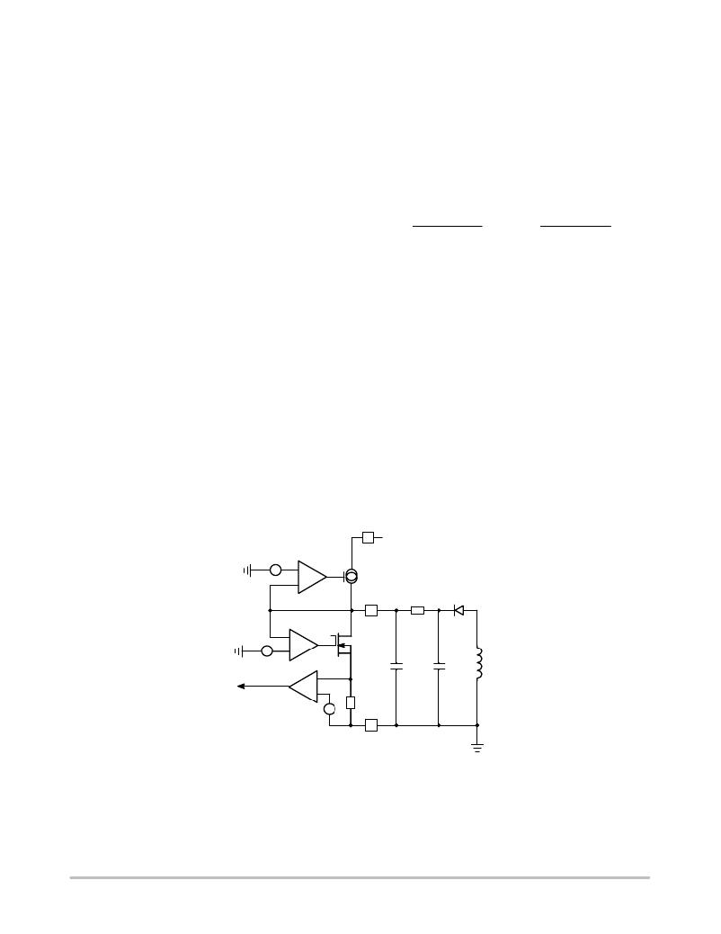
�The� particular� NCP1027� arrangement� offers� a� simple�
�way� to� prevent� output� voltage� runaway� when� the�
�optocoupler� fails.� As� Figure� 34� shows,� an� active� Zener�
�diode� monitors� and� protects� the� V� CC� pin.� Below� its�
�equivalent� breakdown� voltage,� that� is� to� say� 8.7� V� typical,�
�no� current� flows� in� it.� If� the� auxiliary� V� CC� pushes� too� much�
�current� inside� the� Zener,� then� the� controller� considers� an�
�OVP� situation� and� stops� the� pulses.� Figure� 34� shows� that�
�the� insertion� of� a� resistor� (� R� limit� )� between� the� auxiliary� DC�
�standby� (output� unloaded).� Thus,� care� must� be� taken� when�
�calculating� R� limit� 1)� to� not� trigger� the� V� CC� overcurrent� latch�
�(by� injecting� 6.0� mA� into� the� active� clamp� –� always� use� the�
�minimum� value� for� worse� case� design)� in� normal� operation�
�but� 2)� not� to� drop� too� much� voltage� over� R� limit� when�
�entering� standby.� Otherwise,� the� converter� will� enter� burst�
�mode� as� it� will� sense� an� UVLO� condition.� Based� on� these�
�recommendations,� we� are� able� to� bound� R� limit� between� two�
�equations:�
�level� and� the� V� CC� pin� is� mandatory� a)� not� to� damage� the�
�internal� 8.7� V� Zener� diode� during� an� overshoot� for� instance�
�(absolute� maximum� current� is� 15� mA)� b)� to� implement� the�
�Vnom- Vclamp�
�Itrip�
�v� Rlimit� v�
�Vstby- VCCON�
�ICC1�
�(eq.� 3)�
�fail-safe� optocoupler� protection� (OVP)� as� offered� by� the�
�active� clamp.� Please� note� that� there� cannot� be� bad�
�interaction� between� the� clamping� voltage� of� the� internal�
�Zener� and� VCC� ON� since� this� clamping� voltage� is� actually�
�built� on� top� of� VCC� ON� with� a� fixed� amount� of� offset�
�(200� mV� typical).� R� limit� should� be� carefully� selected� to�
�avoid� triggering� the� OVP� as� we� discussed,� but� also� to� avoid�
�disturbing� the� V� CC� in� low/light� load� conditions.� The�
�following� details� how� to� evaluate� the� R� limit� value.�
�Self-supplying� controllers� in� extremely� low� standby�
�applications� often� puzzles� the� designer.� Actually,� if� an�
�SMPS� operated� at� nominal� load� can� deliver� an� auxiliary�
�voltage� of� an� arbitrary� 16� V� (V� nom� ),� this� voltage� can� drop�
�below� 10� V� (V� stby� )� when� entering� standby.� This� is� because�
�the� recurrence� of� the� switching� pulses� expands� so� much,�
�that� the� low� frequency� refueling� rate� of� the� V� CC� capacitor�
�is� not� enough� to� keep� a� proper� auxiliary� voltage.� Figure� 35�
�portrays� a� typical� scope� shot� of� an� SMPS� entering� deep�
�Where:�
�V� nom� is� the� auxiliary� voltage� at� nominal� load.�
�V� stdby� is� the� auxiliary� voltage� when� standby� is� entered.�
�I� trip� is� the� current� corresponding� to� the� nominal� operation.�
�It� thus� must� be� selected� to� avoid� false� tripping� in� overshoot�
�conditions.� Always� use� the� minimum� of� the� specification�
�for� a� robust� design.�
�ICC1� is� the� controller� consumption.� This� number� slightly�
�decreases� compared� to� ICC1� from� the� spec� since� the� part�
�in� standby� does� almost� not� switch.� It� is� around� 1.0� mA� for�
�the� 65� kHz� version.�
�VCC� (min)� is� the� level� above� which� the� auxiliary� voltage�
�must� be� maintained� to� keep� the� controller� away� from� the�
�UVLO� trip� point.� It� is� good� to� obtain� around� 8.0� V� in� order�
�to� offer� an� adequate� design� margin,� e.g.� to� not� reactivate� the�
�startup� source� (which� is� not� a� problem� in� itself� if� low�
�standby� power� does� not� matter).�
�Drain�
�V� CCON� =� 8.5� V�
�V� CC(min)� =� 7.5� V�
�+�
�-�
�+�
�Startup�
�Source�
�+�
�V� CC�
�R� limit�
�D1�
�-�
�+�
�V� clamp� =� 8.7� V� Typ.�
�+�
�C� VCC�
�+�
�C� AUX�
�L� aux�
�Latch�
�+�
�-�
�+�
�I� >� 6� mA�
�Ground�
�Figure� 34.� A� more� detailed� view� of� the� NCP1027� offers� better�
�insight� on� how� to� properly� wire� an� auxiliary� winding.�
�Since� R� limit� shall� not� bother� the� controller� in� standby,� e.g.�
�keep� Vauxiliary� to� around� 8.0� V� (as� selected� above),� we�
�purposely� select� a� Vnom� well� above� this� value.� As�
�explained� before,� experience� shows� that� a� 40%� decrease�
�can� be� seen� on� auxiliary� windings� from� nominal� operation�
�down� to� standby� mode.� Let's� select� a� nominal� auxiliary�
�winding� of� 20� V� to� offer� sufficient� margin� regarding� 8.0� V�
�when� in� standby� (� R� limit� also� drops� voltage� in� standby� …� ).�
�http://onsemi.com�
�19�
�发布紧急采购,3分钟左右您将得到回复。
相关PDF资料
NCP1608BOOSTGEVB
BOARD EVAL NCP1608 100W BOOST
NCP1631PFCGEVB
BOARD DEMO NCP1631 INTERLEAV PFC
NCP1650EVB
BOARD EVAL NCP1650 PFC CTLR
NCP1652L48VGEVB
BOARD EVAL 100W 48V NCP1652 PFC
NCP1653EVB
BOARD EVAL FOR NCP1653
NCP2993FCT2GEVB
BOARD EVAL NCP2993 AUDIO PWR AMP
NCP345SNT1G
IC DETECTOR OVER VOLTAGE 5TSOP
NCP346SN2T1G
IC DETECTOR OVER VOLTAGE 5TSOP
相关代理商/技术参数
NCP1606ADR2G
功能描述:功率因数校正 IC PWR FCTR CONTROLLER RoHS:否 制造商:Fairchild Semiconductor 开关频率:300 KHz 最大功率耗散: 最大工作温度:+ 125 C 安装风格:SMD/SMT 封装 / 箱体:SOIC-8 封装:Reel
NCP1606APG
功能描述:功率因数校正 IC LO CST PWR FCTR CONT RoHS:否 制造商:Fairchild Semiconductor 开关频率:300 KHz 最大功率耗散: 最大工作温度:+ 125 C 安装风格:SMD/SMT 封装 / 箱体:SOIC-8 封装:Reel
NCP1606BDR2G
功能描述:功率因数校正 IC PWR FCTR CONTROLLER RoHS:否 制造商:Fairchild Semiconductor 开关频率:300 KHz 最大功率耗散: 最大工作温度:+ 125 C 安装风格:SMD/SMT 封装 / 箱体:SOIC-8 封装:Reel
NCP1606BOOSTGEVB
功能描述:电源管理IC开发工具 OSPI NCP1606 100 W BOOST
RoHS:否 制造商:Maxim Integrated 产品:Evaluation Kits 类型:Battery Management 工具用于评估:MAX17710GB 输入电压: 输出电压:1.8 V
NCP1606BPG
功能描述:功率因数校正 IC LO CST PWR FCTR CONT RoHS:否 制造商:Fairchild Semiconductor 开关频率:300 KHz 最大功率耗散: 最大工作温度:+ 125 C 安装风格:SMD/SMT 封装 / 箱体:SOIC-8 封装:Reel
NCP1607BDR2G
功能描述:功率因数校正 IC CST EFCT PW FCTR CTR RoHS:否 制造商:Fairchild Semiconductor 开关频率:300 KHz 最大功率耗散: 最大工作温度:+ 125 C 安装风格:SMD/SMT 封装 / 箱体:SOIC-8 封装:Reel
NCP1607BOOSTGEVB
功能描述:BOARD EVAL NCP1607 100W BOOST RoHS:是 类别:编程器,开发系统 >> 评估演示板和套件 系列:* 标准包装:1 系列:PCI Express® (PCIe) 主要目的:接口,收发器,PCI Express 嵌入式:- 已用 IC / 零件:DS80PCI800 主要属性:- 次要属性:- 已供物品:板
NCP1608BDR2G
功能描述:功率因数校正 IC COST EFFECT PWR FACT CONT RoHS:否 制造商:Fairchild Semiconductor 开关频率:300 KHz 最大功率耗散: 最大工作温度:+ 125 C 安装风格:SMD/SMT 封装 / 箱体:SOIC-8 封装:Reel